Power divider
34~54GHz, 1W, 2way, Phase0°
- ZPD8-2M34-54G-2551
- China
- One Year
- +86-19938031308
- sales@com-mw.com, cynthia@com-mw.com
- 3-1-2306, No.37 Jiancai Road, Chenghua Zone, Chengdu
- For qty details, please search in spot products of dianzibuy. Any changes to the contents are not notified. Please confirm again before ordering.
- No restrictions on export to any country
- RoHS compliant (Meet RoHS standards can be customized)
Product Details
Main specifications
| Parameters | Min | Typical | Max | Units |
| Frequency | 34 | ~ | 54 | GHz |
| IL | 0.8 | dB | ||
| Isolation | 20 | dB | ||
| Input VSWR | 1.5 | |||
| Output VSWR | 1.5 | |||
| Amplitude balance | 0.4 | dB | ||
| Phase balance | ±6 | ° |
Other parameters
| Power | 1W Design assurance |
| way | 2-way |
| Phase | 0° |
| Impedance | 50Ω |
| Connector | Microstrip pad |
| Work Temp. | -40~+85℃ Design assurance |
| Other | Thin film ceramics |
Port Definition
| Common port | 0 |
| Dispatch Port | 1,2 |
Suggested PCB Layout
Typical test data
| Frequency(GHz) | S11 VSWR | S12 Loss dB | S13 IL dB | S23 Rejection | S13 Phase (°) |
| 32.14 | 1.27 | -4.21 | -4.09 | -17.31 | 0.56 |
| 34.29 | 1.05 | -3.34 | -3.39 | -19.46 | |
| 36.43 | 1.17 | -3.4 | -3.22 | -21.03 | 0.39 |
| 38.57 | 1.19 | -3.32 | -3.22 | -23.44 | -1.98 |
| 40.71 | 1.42 | -3.63 | -3.69 | -28.12 | -2.31 |
| 42.86 | 1.4 | -3.48 | -3.73 | -25.64 | -2.67 |
| 45 | 1.45 | -3.61 | -3.72 | -25.57 | -1.41 |
| 47.14 | 1.49 | -3.63 | -3.56 | -27.97 | -3.45 |
| 49.29 | 1.39 | -3.37 | -3.52 | -26.87 | -3.91 |
| 51.43 | 1.27 | -3.47 | -3.56 | -23.45 | -4.57 |
| 53.57 | 1.33 | -3.36 | -3.56 | -22.87 | -4.41 |
| 55.71 | 1.71 | -3.81 | -4.02 | -30.34 | -4.38 |
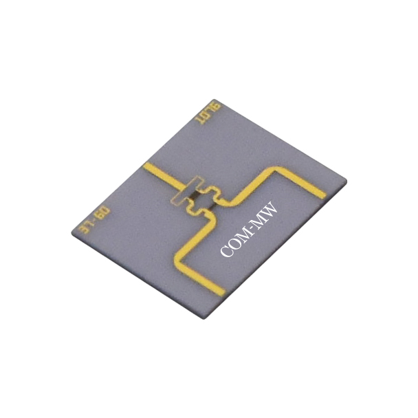
Reference picture

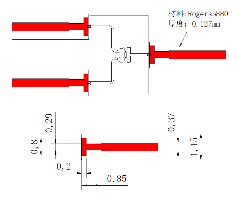
Configuration(mm)

Typical test curve

Note
| 1 | The chip is recommended to be used in separate cavities, with a distance of 0.1mm from the sidewall on one side and a distance of 1-2mm from the upper cover on the surface. |
| 2 | Low stress conductive adhesive (ME8456) is recommended for bonding chips. |
| 3 | The chip should be installed on a carrier such as molybdenum copper, which is close to the thermal expansion coefficient of ceramics (6.7ppm/C °), with a carrier thickness of ≥ 0.2mm. |
| 4 | When the Microstrip of the circuit board is bonded to the chip, it is recommended to use a T-shaped structure at the microstrip bonding point for matching. |